Computer Organization and Architecture – Memory Organisation
Concept of Memory
We have already mentioned that digital computer works on stored programmed concept introduced by Von Neumann. We use memory to store the information, which includes both program and data.
Due to several reasons, we have different kind of memories. We use different kind of memory at different lavel.The memory of computer is broadly categories into two categories: Internal and external.
Internal memory is used by CPU to perform task and external memory is used to store bulk information, which includes large software and data.
Memory is used to store the information in digital form.
The memory hierarchy is given by:
- Register
- Cache Memory
- Main Memory
- Magnetic Disk
- Removable media (Magnetic tape)
Register:
This is a part of Central Processor Unit, so they reside inside the CPU. The information from main memory is brought to CPU and keep the information in register. Due to space and cost constraints, we have got a limited number of registers in a CPU. These are basically faster devices.
Cache Memory:
Cache memory is a storage device placed in between CPU and main memory. These are semiconductor memories. These are basically fast memory device, faster than main memory.
We can not have a big volume of cache memory due to its higher cost and some constraints of the CPU. Due to higher cost we can not replace the whole main memory by faster memory. Generally, the most recently used information is kept in the cache memory. It is brought from the main memory and placed in the cache memory. Now a days, we get CPU with internal cache.
Main Memory:
Like cache memory, main memory is also semiconductor memory. But the main memory is relatively slower memory. We have to first bring the information (whether it is data or program), to main memory. CPU can work with the information available in main memory only.
Magnetic Disk:
This is bulk storage device. We have to deal with huge amount of data in many application. But we don’t have so much semiconductor memory to keep these information in our computer. On the other hand, semiconductor memories are volatile in nature. It loses its content once we switch off the computer. For permanent storage, we use magnetic disk. The storage capacity of magnetic disk is very high.
Removable media:
For different application, we use different data. It may not be possible to keep all the information in magnetic disk. So, which ever data we are not using currently, can be kept in removable media. Magnetic tape is one kind of removable medium. CD is also a removable media, which is an optical device.
Register, cache memory and main memory are internal memory. Magnetic Disk, removable media are external memory. Internal memories are semiconductor memory. Semiconductor memories are categoried as volatile memory and non-volatile memory.
RAM: Random Access Memories are volatile in nature. As soon as the computer is switched off, the contents of memory are also lost.
ROM: Read only memories are non volatile in nature. The storage is permanent, but it is read only memory. We can not store new information in ROM.
Several types of ROM are available:
PROM: Programmable Read Only Memory; it can be programmed once as per user requirements.
EPROM: Erasable Programmable Read Only Memory; the contents of the memory can be erased and store new data into the memory. In this case, we have to erase whole information.
EEPROM: Electrically Erasable Programmable Read Only Memory; in this type of memory the contents of a particular location can be changed without effecting the contents of other location.
Main Memory
The main memory of a computer is semiconductor memory. The main memory unit of computer is basically consists of two kinds of memory:
RAM : Random access memory; which is volatile in nature.
ROM : Read only memory; which is non-volatile.
The permanent information are kept in ROM and the user space is basically in RAM.
The smallest unit of information is known as bit (binary digit), and in one memory cell we can store one bit of information. 8 bit together is termed as a byte.
The maximum size of main memory that can be used in any computer is determined by the addressing scheme.
A computer that generates 16-bit address is capable of addressing upto 216 which is equal to 64K memory location. Similarly, for 32 bit addresses, the total capacity will be 232 which is equal to 4G memory location.
In some computer, the smallest addressable unit of information is a memory word and the machine is called word-addressable.
In some computer, individual address is assigned for each byte of information, and it is called byte-addressable computer. In this computer, one memory word contains one or more memory bytes which can be addressed individually.
A byte addressable 32-bit computer, each memory word contains 4 bytes. A possible way of address assignment is shown in figure. The address of a word is always integer multiple of 4.
The main memory is usually designed to store and retrieve data in word length quantities. The word length of a computer is generally defined by the number of bits actually stored or retrieved in one main memory access.
Consider a machine with 32 bit address bus. If the word size is 32 bit, then the high order 30 bit will specify the address of a word. If we want to access any byte of the word, then it can be specified by the lower two bit of the address bus.
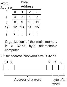 Address assignment to a 4-byte word
The data transfer between main memory and the CPU takes place through two CPU registers.
MAR : Memory Address Register
MDR : Memory Data Register.
If the MAR is k-bit long, then the total addressable memory location will be 2k.
If the MDR is n-bit long, then the n bit of data is transferred in one memory cycle.
The transfer of data takes place through memory bus, which consist of address bus and data bus. In the above example, size of data bus is n-bit and size of address bus is k bit.
It also includes control lines like Read, Write and Memory Function Complete (MFC) for coordinating data transfer. In the case of byte addressable computer, another control line to be added to indicate the byte transfer instead of the whole word.
For memory operation, the CPU initiates a memory operation by loading the appropriate data i.e., address to MAR.
If it is a memory read operation, then it sets the read memory control line to 1. Then the contents of the memory location is brought to MDR and the memory control circuitry indicates this to the CPU by setting MFC to 1.
If the operation is a memory write operation, then the CPU places the data into MDR and sets the write memory control line to 1. Once the contents of MDR are stored in specified memory location, then the memory control circuitry indicates the end of operation by setting MFC to 1.
A useful measure of the speed of memory unit is the time that elapses between the initiation of an operation and the completion of the operation (for example, the time between Read and MFC). This is referred to as Memory Access Time. Another measure is memory cycle time. This is the minimum time delay between the initiation two independent memory operations (for example, two successive memory read operation). Memory cycle time is slightly larger than memory access time.
Binary Storage Cell:
The binary storage cell is the basic building block of a memory unit.
The binary storage cell that stores one bit of information can be modelled by an SR latch with associated gates.
1 bit Binary Cell (BC)
The binary cell stores one bit of information in its internal latch.
Control input to binary cell
Select Read/Write Memory Operation
0 X None
1 0 Write
1 1 Read
The storage part is modeled here with SR-latch, but in reality it is an electronics circuit made up of transistors.
The memory constructed with the help of transistors is known as semiconductor memory. The semiconductor memories are termed as Random Access Memory(RAM), because it is possible to access any memory location in random.
Depending on the technology used to construct a RAM, there are two types of RAM –
SRAM: Static Random Access Memory.
DRAM: Dynamic Random Access Memory.
Dynamic Ram (DRAM):
A DRAM is made with cells that store data as charge on capacitors. The presence or absence of charge in a capacitor is interpreted as binary 1 or 0.
Because capacitors have a natural tendency to discharge due to leakage current, dynamic RAM require periodic charge refreshing to maintain data storage. The term dynamic refers to this tendency of the stored charge to leak away, even with power continuously applied.
For the write operation, a voltage signal is applied to the bit line B, a high voltage represents 1 and a low voltage represents 0. A signal is then applied to the address line, which will turn on the transistor T, allowing a charge to be transferred to the capacitor.
For the read operation, when a signal is applied to the address line, the transistor T turns on and the charge stored on the capacitor is fed out onto the bit line B and to a sense amplifier.
The sense amplifier compares the capacitor voltage to a reference value and determines if the cell contains a logic 1 or a logic 0.
The read out from the cell discharges the capacitor, width must be restored to complete the read operation.
Due to the discharge of the capacitor during read operation, the read operation of DRAM is termed as destructive read out.
Static RAM (SRAM):
In an SRAM, binary values are stored using traditional flip-flop constructed with the help of transistors. A static RAM will hold its data as long as power is supplied to it.
SRAM Versus DRAM :
Both static and dynamic RAMs are volatile, that is, it will retain the information as long as power supply is applied.
A dynamic memory cell is simpler and smaller than a static memory cell. Thus a DRAM is more dense,
i.e., packing density is high(more cell per unit area). DRAM is less expensive than corresponding SRAM.
DRAM requires the supporting refresh circuitry. For larger memories, the fixed cost of the refresh circuitry is more than compensated for by the less cost of DRAM cells
SRAM cells are generally faster than the DRAM cells. Therefore, to construct faster memory modules(like cache memory) SRAM is used.
Cache Memory
Analysis of large number of programs has shown that a number of instructions are executed repeatedly. This may be in the form of a simple loops, nested loops, or a few procedures that repeatedly call each other. It is observed that many instructions in each of a few localized areas of the program are repeatedly executed, while the remainder of the program is accessed relatively less. This phenomenon is referred to as locality of reference.
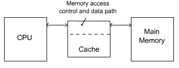
Now, if it can be arranged to have the active segments of a program in a fast memory, then the tolal execution time can be significantly reduced. It is the fact that CPU is a faster device and memory is a relatively slower device. Memory access is the main bottleneck for the performance efficiency. If a faster memory device can be inserted between main memory and CPU, the efficiency can be increased. The faster memory that is inserted between CPU and Main Memory is termed as Cache memory.
To make this arrangement effective, the cache must be considerably faster than the main memory, and typically it is 5 to 10 time faster than the main memory. This approach is more economical than the use of fast memory device to implement the entire main memory. This is also a feasible due to the locality of reference that is present in most of the program, which reduces the frequent data transfer between main memory and cache memory.
Operation of Cache Memory
- The memory control circuitry is designed to take advantage of the property of locality of reference. Some assumptions are made while designing the memory control circuitry:
- The CPU does not need to know explicitly about the existence of the cache.
- The CPU simply makes Read and Write request. The nature of these two operations are same whether cache is present or not.
- The address generated by the CPU always refer to location of main memory.
- The memory access control circuitry determines whether or not the requested word currently exists in the cache. When a Read request is received from the CPU, the contents of a block of memory words containing the location specified are transferred into the cache. When any of the locations in this block is referenced by the program, its contents are read directly from the cache.
Consider the case where the addressed word is not in the cache and the operation is a read. First the block of words is brought to the cache and then the requested word is forwarded to the CPU. But it can be forwarded to the CPU as soon as it is available to the cache, instaead of the whole block to be loaded in the cache. This is called load through, and there is some scope to save time while using load through policy. - The cache memory can store a number of such blocks at any given time.
- The correspondence between the Main Memory Blocks and those in the cache is specified by means of a mapping function.
When the cache is full and a memory word is referenced that is not in the cache, a decision must be made as to which block should be removed from the cache to create space to bring the new block to the cache that contains the referenced word. Replacement algorithms are used to make the proper selection of block that must be replaced by the new one. - When a write request is received from the CPU, there are two ways that the system can proceed. In the first case, the cache location and the main memory location are updated simultaneously. This is called the store through method or write through method.
- The alternative is to update the cache location only. During replacement time, the cache block will be written back to the main memory. This method is called write back method. If there is no new write operation in the cache block, it is not required to write back the cache block in the main memory. This information can be kept with the help of an associated bit. This bit it set while there is a write operation in the cache block. During replacement, it checks this bit, if it is set, then write back the cache block in main memory otherwise not. This bit is known as dirty bit. If the bit gets dirty (set to one), writting to main memory is required.
- The write through method is simpler, but it results in unnecessary write operations in the main memory when a given cache word is updated a number of times during its cache residency period.
During a write operation, if the address word is not in the cache, the information is written directly into the main memory. A write operation normally refers to the location of data areas and the property of locality of reference is not as pronounced in accessing data when write operation is involved. Therefore, it is not advantageous to bring the data block to the cache when there a write operation, and the addressed word is not present in cache.
For Offline Study you can Download pdf file from below link
Download Computer Organization and Architecture Memory Organisation PDF File