8086 Microprocessor – General Bus Operation Cycle Minimum Mode and Maximum Mode
General Bus Operation Cycle Overview
The 8086 microprocessor supports two modes of operation, Minimum Mode and Maximum Mode. Both modes involve a bus operation cycle, which is the sequence of steps that the microprocessor follows to read or write data from or to an external device. Here is an overview of the bus operation cycle in each mode:
- Minimum Mode:
In Minimum Mode, the 8086 microprocessor is used in simple systems that require only one microprocessor to control the bus. In this mode, the microprocessor generates all the control signals required for bus operations. The bus operation cycle in Minimum Mode consists of the following steps:
- Address Setup: The microprocessor places the address of the memory location or I/O device on the address bus during the first clock cycle.
- Address Hold: The address bus is held steady while the memory or I/O device decodes the address and prepares for data transfer.
- Read or Write: The microprocessor generates a Read or Write signal during the third clock cycle, depending on whether it is reading or writing data.
- Data Transfer: During the next clock cycle, data is transferred between the microprocessor and the memory or I/O device.
- Bus Release: The bus is released after the data transfer is complete.
- Maximum Mode:
In Maximum Mode, the 8086 microprocessor is used in more complex systems that require multiple microprocessors or other devices to share the bus. In this mode, the microprocessor generates the Minimum Mode control signals, but also uses a bus controller to manage the bus. The bus operation cycle in Maximum Mode consists of the following steps:
- Bus Request: A device that wants to use the bus sends a Bus Request signal to the bus controller.
- Bus Grant: The bus controller grants access to the bus to the requesting device.
- Address Setup: The requesting device places the address of the memory location or I/O device on the address bus during the first clock cycle.
- Address Hold: The address bus is held steady while the memory or I/O device decodes the address and prepares for data transfer.
- Read or Write: The requesting device generates a Read or Write signal during the third clock cycle, depending on whether it is reading or writing data.
- Data Transfer: During the next clock cycle, data is transferred between the requesting device and the memory or I/O device.
- Bus Release: The requesting device releases the bus after the data transfer is complete.
Overall, the bus operation cycle is a critical aspect of the operation of the 8086 microprocessor. By understanding the steps involved in the bus operation cycle in both Minimum Mode and Maximum Mode, students can gain a deeper understanding of how the microprocessor interacts with the external devices in a computer system.
General Bus Operation:
- The 8086 has a combined address and data bus commonly referred as a time multiplexed address and data bus.
- The main reason behind multiplexing address and data over the same pins is the maximum utilisation of processor pins and it facilitates the use of 40 pin standard DIP package.
- The bus can be demultiplexed using a few latches and trans-receivers, when ever required.
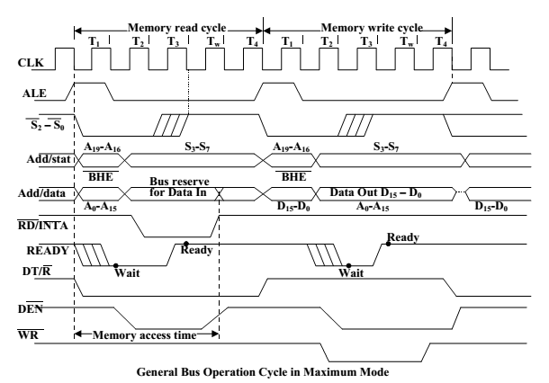
- Basically, all the processor bus cycles consist of at least four clock cycles. These are referred to as T1, T2, T3, T4. The address is transmitted by the processor during T1. It is Present on the bus only for one cycle.
- The negative edge of this ALE pulse is used to separate the address and the data or status information. In maximum mode, the status lines S0, S1 and S2 are used to indicate the
Type of operation.
- Status bits S3 to S7 are multiplexed with higher order address bits and the BHE signal. Address is valid during T1 while status bits S3 to S7 are valid during T2 through T4.
Minimum Mode 8086 System
In this mode, all the control signals are given out by the microprocessor chip itself. There is a single microprocessor in the minimum mode system.
In a minimum mode 8086 system, the microprocessor 8086 is operated in minimum mode by strapping its MN/MX pin to logic 1.
The remaining components in the system are latches, transreceivers, clock generator, memory and I/O devices. Some type of chip selection logic may be required for selecting memory or I/O devices, depending upon the address map of the system.
Latches are generally buffered output D-type flip-flops like 74LS373 or 8282. They are used for separating the valid address from the multiplexed address/data signals and are controlled by the ALE signal generated by 8086.
Transreceivers are the bidirectional buffers and some times they are called as data amplifiers. They are required to separate the valid data from the time multiplexed address/data signals.
They are controlled by two signals namely, DEN and DT/R. The DEN signal indicates the direction of data, i.e. from or to the processor. The system contains memory for the monitor and users program storage.
Usually, EPROM are used for monitor storage, while RAM for users program storage. A system may contain I/O devices.
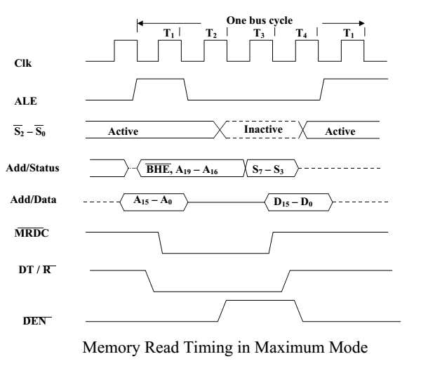
The working of the minimum mode configuration system can be better described in terms of the timing diagrams rather than qualitatively describing the operations. •The opcode fetch and read cycles are similar. Hence the timing diagram can be categorized in two parts, the first is the timing diagram for read cycle and the second is the timing diagram for write cycle.
The read cycle begins in T1 with the assertion of address latch enable (ALE) signal and also M / IO signal. During the negative going edge of this signal, the valid address is latched on the local bus.
The BHE and A0 signals address low, high or both bytes. From T1 to T4 , the M/IO signal indicates a memory or I/O operation.
At T2, the address is removed from the local bus and is sent to the output. The bus is then tristated. The read (RD) control signal is also activated in T2.
The read (RD) signal causes the address device to enable its data bus drivers. After RD goes low, the valid data is available on the data bus.
The addressed device will drive the READY line high. When the processor returns the read signal to high level, the addressed device will again tristate its bus drivers.
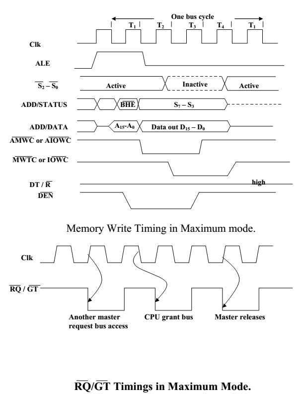
A write cycle also begins with the assertion of ALE and the emission of the address. The M/IO signal is again asserted to indicate a memory or I/O operation. In T2, after sending the address in T1, the processor sends the data to be written to the addressed location. •The data remains on the bus until middle of T4 state. The WR becomes active at the beginning of T2 (unlike RD is somewhat delayed in T2 to provide time for floating).
The BHE and A0 signals are used to select the proper byte or bytes of memory or I/O word to be read or write.
The M/IO, RD and WR signals indicate the type of data transfer as specified in table below

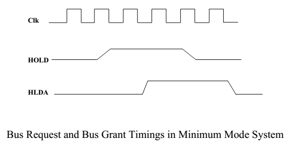
Hold Response sequence: The HOLD pin is checked at leading edge of each clock pulse. If it is received active by the processor before T4 of the previous cycle or during T1 state of the current cycle, the CPU activates HLDA in the next clock cycle and for succeeding bus cycles, the bus will be given to another requesting master.
The control of the bus is not regained by the processor until the requesting master does not drop the HOLD pin low. When the request is dropped by the requesting master, the HLDA is dropped by the processor at the trailing edge of the next clock.
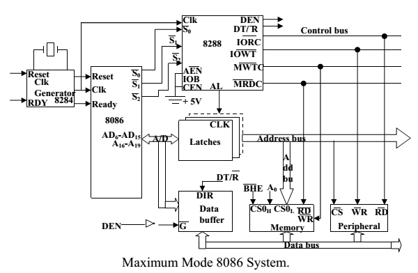
Maximum Mode 8086 System
In the maximum mode, the 8086 is operated by strapping the MN/MX pin to ground.
In this mode, the processor derives the status signal S2, S1, S0. Another chip called bus controller derives the control signal using this status information.
In the maximum mode, there may be more than one microprocessor in the system configuration.
The components in the system are same as in the minimum mode system.
The basic function of the bus controller chip IC8288, is to derive control signals like RD and WR ( for memory and I/O devices), DEN, DT/R, ALE etc. using the information by the processor on the status lines.
The bus controller chip has input lines S2, S1, S0 and CLK. These inputs to 8288 are driven by CPU.
It derives the outputs ALE, DEN, DT/R, MRDC, MWTC, AMWC, IORC, IOWC and AIOWC. The AEN, IOB and CEN pins are specially useful for multiprocessor systems. •AEN and IOB are generally grounded. CEN pin is usually tied to +5V. The significance of the MCE/PDEN output depends upon the status of the IOB pin.
If IOB is grounded, it acts as master cascade enable to control cascade 8259A, else it acts as peripheral data enable used in the multiple bus configurations.
INTA pin used to issue two interrupt acknowledge pulses to the interrupt controller or to an interrupting device.
IORC, IOWC are I/O read command and I/O write command signals respectively. These signals enable an IO interface to read or write the data from or to the address port.
The MRDC, MWTC are memory read command and memory write command signals respectively and may be used as memory read or write signals.
All these command signals instructs the memory to accept or send data from or to the bus.
For both of these write command signals, the advanced signals namely AIOWC and AMWTC are available.
Here the only difference between in timing diagram between minimum mode and maximum mode is the status signals used and the available control and advanced command signals.
R0, S1, S2 are set at the beginning of bus cycle.8288 bus controller will output a pulse as on the ALE and apply a required signal to its DT / R pin during T1.
In T2, 8288 will set DEN=1 thus enabling transceivers, and for an input it will activate MRDC or IORC. These signals are activated until T4. For an output, the AMWC or AIOWC is activated from T2 to T4 and MWTC or IOWC is activated from T3 to T4. •The status bit S0 to S2 remains active until T3 and become passive during T3 and T 4.
If reader input is not activated before T3, wait state will be inserted between T3 and T4.
Timings for RQ/ GT Signals:
The request/grant response sequence contains a series of three pulses. The request/grant pins are checked at each rising pulse of clock input.
When a request is detected and if the condition for HOLD request are satisfied, the processor issues a grant pulse over the RQ/GT pin immediately during T4 (current) or T1 (next) state.
When the requesting master receives this pulse, it accepts the control of the bus, it sends a release pulse to the processor using RQ/GT pin.
Minimum Mode Interface
When the Minimum mode operation is selected, the 8086 provides all control signals needed to implement the memory and I/O interface.
The minimum mode signal can be divided into the following basic groups: address/data bus, status, control, interrupt and DMA.
Address/Data Bus: these lines serve two functions. As an address bus is 20 bits long and consists of signal lines A0 through A19. A19 represents the MSB and A0 LSB. A 20bit address gives the 8086 a 1Mbyte memory address space. More over it has an independent I/O address space which is 64K bytes in length.
The 16 data bus lines D0 through D15 are actually multiplexed with address lines A0 through A15 respectively. By multiplexed we mean that the bus work as an address bus during first machine cycle and as a data bus during next machine cycles. D15 is the MSB and D0 LSB.
When acting as a data bus, they carry read/write data for memory, input/output data for I/O devices, and interrupt type codes from an interrupt controller.
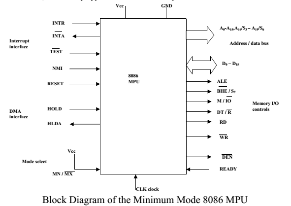
Status signal:
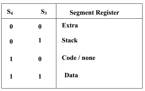
The four most significant address lines A19 through A16 are also multiplexed but in this case with status signals S6 through S3. These status bits are output on the bus at the same time that data are transferred over the other bus lines.
Bit S4 and S3 together from a 2 bit binary code that identifies which of the 8086 internal segment registers are used to generate the physical address that was output on the address bus during the current bus cycle.
Code S4S3 = 00 identifies a register known as extra segment register as the source of the segment address.
Status line S5 reflects the status of another internal characteristic of the 8086. It is the logic level of the internal enable flag. The last status bit S6 is always at the logic 0 level.