8086 Microprocessor – Internal Architecture of 8086
Overview of the main components
The internal architecture of the 8086 microprocessor consists of various components that work together to execute instructions and process data. Here is an overview of the main components:
- Registers: The 8086 has 14 registers, including four 16-bit general-purpose registers (AX, BX, CX, and DX), four 16-bit index registers (SI, DI, BP, and SP), and six segment registers (CS, DS, SS, ES, FS, and GS). The registers are used to store data and addresses.
- Execution unit: The execution unit is responsible for executing instructions. It includes an arithmetic logic unit (ALU) that performs arithmetic and logic operations, and a barrel shifter that shifts bits left or right.
- Control unit: The control unit coordinates the operations of the microprocessor. It includes a decoder that interprets instructions, and a bus interface unit that communicates with external devices.
- Memory: The 8086 uses a segmented memory model, which divides memory into segments that are up to 64KB in size. Each segment is identified by a segment register, and the offset within the segment is stored in a general-purpose register or index register.
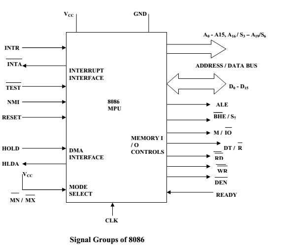
- Address bus and data bus: The address bus is used to send addresses to memory and other devices, while the data bus is used to send and receive data.
- Interrupt controller: The interrupt controller manages interrupts, which are signals that indicate that a device needs attention from the processor.
- Clock generator: The clock generator provides the clock signal that synchronizes the operations of the microprocessor.
Overall, the internal architecture of the 8086 microprocessor is complex, but it provides a powerful platform for executing instructions and processing data. By understanding the internal architecture of the 8086, you can gain a deeper understanding of how microprocessors work and how they are used in computer systems.
The 8086 microprocessor contains two main units, the Bus Interface Unit (BIU) and the Execution Unit (EU). Here’s a brief overview of each unit and its functions:
- Bus Interface Unit (BIU): The BIU is responsible for managing the external bus interface of the microprocessor. Its functions include fetching instructions from memory, generating physical memory addresses, controlling the external bus, and handling interrupts.
- Execution Unit (EU): The EU is responsible for executing instructions that are fetched by the BIU. Its functions include performing arithmetic and logic operations, shifting and rotating bits, and controlling program flow through conditional and unconditional jumps.
The BIU and EU work together to execute instructions and process data. The BIU fetches instructions from memory and stores them in the instruction queue, while the EU executes the instructions in the queue. The BIU also generates physical memory addresses that are used by the EU to access data in memory or I/O devices. The EU performs arithmetic and logic operations on data, stores results in registers, and controls program flow through jumps and branches.
The separation of the BIU and EU allows for parallel processing of instructions, which improves the overall performance of the microprocessor. The BIU can fetch and queue instructions while the EU is executing instructions from the queue, which helps to reduce the time required to fetch and execute instructions.
Bus Interface Unit (BIU)
The Bus Interface Unit (BIU) is one of the main components of the 8086 microprocessor. It is responsible for managing the external bus interface, which connects the microprocessor to memory and other devices. Here’s an overview of the BIU and its functions:
- Instruction queue: The BIU contains a 6-byte instruction queue that holds up to six instruction bytes. This allows the BIU to fetch multiple instructions in advance and store them in the queue, which helps to improve the performance of the microprocessor.
- Instruction pointer: The BIU also contains a 16-bit instruction pointer (IP) register, which points to the next instruction in memory to be executed. When the BIU fetches an instruction, it increments the IP to point to the next instruction in memory.
- Address generation: The BIU generates the 20-bit physical memory address for memory and I/O operations. The address is generated by combining the segment address from the appropriate segment register (CS, DS, ES, SS, FS, or GS) and the offset address from one of the general-purpose registers (BX, BP, SI, or DI).
- Bus control: The BIU controls the external bus interface by generating the necessary control signals. These signals include the address strobe (ADS) signal, which indicates that the address on the address bus is valid; the data strobe (DS) signal, which indicates that data on the data bus is valid; and the read/write (R/W) signal, which indicates whether the operation is a read or write operation.
- Interrupt handling: The BIU also manages interrupts by monitoring the interrupt request (INT) and non-maskable interrupt (NMI) signals. When an interrupt is detected, the BIU saves the current instruction pointer and the flags register on the stack, and transfers control to the interrupt service routine.
Overall, the BIU is an important component of the 8086 microprocessor that manages the external bus interface and controls the flow of data and instructions between the microprocessor and external devices. Its functions are critical to the overall operation of the microprocessor.
Execution Unit (EU)
The Execution Unit (EU) is one of the main units of the 8086 microprocessor, responsible for executing instructions that are fetched by the Bus Interface Unit (BIU). The EU contains several components that work together to execute instructions and process data. Here is an overview of the main components of the EU:
- Arithmetic Logic Unit (ALU): The ALU is responsible for performing arithmetic and logic operations on data. It can perform operations such as addition, subtraction, multiplication, division, AND, OR, XOR, and NOT. The ALU also sets the flags register based on the result of the operation.
- General-Purpose Registers: The EU contains several general-purpose registers that are used to store data and addresses. The AX, BX, CX, and DX registers are each 16 bits wide and can be used for various purposes, such as holding data for arithmetic operations or addresses for memory access. The SI, DI, BP, and SP registers are also 16 bits wide and are used for specific purposes such as indexing data or holding the stack pointer.
- Flags Register: The flags register is a 16-bit register that contains status flags that are set by the ALU based on the result of arithmetic and logic operations. The flags indicate conditions such as whether the result is zero, negative, or overflowed. The flags register is used by conditional jump instructions to control program flow.
- Barrel Shifter: The barrel shifter is a component that can shift or rotate the bits in a register left or right. This is useful for operations such as multiplication and division, as well as for bit manipulation operations.
- Instruction Decoder: The instruction decoder is responsible for interpreting the instructions that are fetched from memory by the BIU. It determines the operation code (opcode) and any operands that are required by the instruction.
- Control Unit: The control unit coordinates the operations of the EU and ensures that instructions are executed in the correct order. It controls program flow through jumps and branches, and manages the flow of data between registers and memory.
Overall, the Execution Unit is a complex component of the 8086 microprocessor that performs a wide range of operations on data and instructions. By understanding the functions of the EU, students can gain a deeper understanding of how microprocessors work and how they are used in computer systems.
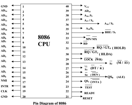
Features
- It is a 16-bit µp.
- 8086 has a 20 bit address bus can access up to 220 memory locations (1 MB).
- It can support up to 64K I/O ports.
- It provides 14, 16 -bit registers.
- It has multiplexed address and data bus AD0- AD15 and A16 – A19.
- It requires single phase clock with 33% duty cycle to provide internal timing.
- 8086 is designed to operate in two modes, Minimum and Maximum.
- It can prefetches upto 6 instruction bytes from memory and queues them in order to speed up instruction execution.
- It requires +5V power supply.
- A 40 pin dual in line package
- Address ranges from 00000H to FFFFFH
Minimum and Maximum Modes:
• The minimum mode is selected by applying logic 1 to the MN / MX input pin. This is a single microprocessor configuration.
• The maximum mode is selected by applying logic 0 to the MN / MX input pin. This is a multi micro processors configuration.
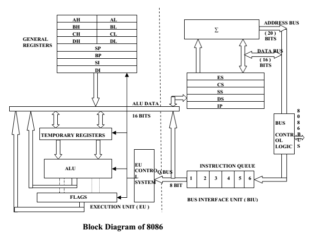
Internal Architecture of 8086
- 8086 has two blocks BIU and EU.
- The BIU performs all bus operations such as instruction fetching, reading and writing operands for memory and calculating the addresses of the memory operands. The instruction bytes are transferred to the instruction queue.
- EU executes instructions from the instruction system byte queue.
- Both units operate asynchronously to give the 8086 an overlapping instruction fetch and execution mechanism which is called as Pipelining. This results in efficient use of the system bus and system performance.
- BIU contains Instruction queue, Segment registers, Instruction pointer, Address adder.
- EU contains Control circuitry, Instruction decoder, ALU, Pointer and Index register, Flag register.