8086 Microprocessor – Bus Interface Unit,Execution Unit
Bus Interface Unit:
It provides a full 16 bit bidirectional data bus and 20 bit address bus.
The bus interface unit is responsible for performing all external bus operations. Specifically it has the following functions:
- Instruction fetch
- Instruction queuing
- Operand fetch and storage
- Address relocation
- Bus control.
The BIU uses a mechanism known as an instruction stream queue to implement a pipeline architecture.
This queue permits prefetch of up to six bytes of instruction code. When ever the queue of the BIU is not full, it has room for at least two more bytes and at the same time the EU is not requesting it to read or write operands from memory, the BIU is free to look ahead in the program by prefetching the next sequential instruction.
These prefetching instructions are held in its FIFO queue. With its 16 bit data bus, the BIU fetches two instruction bytes in a single memory cycle.
After a byte is loaded at the input end of the queue, it automatically shifts up through the FIFO to the empty location nearest the output.
The EU accesses the queue from the output end. It reads one instruction byte after the other from the output of the queue. If the queue is full and the EU is not requesting access to operand in memory.
These intervals of no bus activity, which may occur between bus cycles are known as Idle state.
If the BIU is already in the process of fetching an instruction when the EU request it to read or write operands from memory or I/O, the BIU first completes the instruction fetch bus cycle before initiating the operand read / write Cycle.
The BIU also contains a dedicated adder which is used to generate the 20bit physical address that is output on the address bus. This address is formed by adding an appended 16 bit segment address and a 16 bit offset address.
For example: The physical address of the next instruction to be fetched is formed by combining the current contents of the code segment CS register and the current contents of the instruction pointer IP register.
The BIU is also responsible for generating bus control signals such as those for memory read or write and I/O read or write.
Execution Unit
The Execution unit is responsible for decoding and executing all instructions.
The EU extracts instructions from the top of the queue in the BIU, decodes them,generates operands if necessary, passes them to the BIU and requests it to perform the read or write bys cycles to memory or I/O and perform the operation specified by the instruction on the operands.
During the execution of the instruction, the EU tests the status and control flags and updates them based on the results of executing the instruction.If the queue is empty, the EU waits for the next instruction byte to be fetched and shifted to top of the queue.
When the EU executes a branch or jump instruction, it transfers control to a location corresponding to another set of sequential instructions.Whenever this happens, the BIU automatically resets the queue and then begins to fetch instructions from this new location to refill the queue.
The Microprocessor 8086 is a 16-bit CPU available in different clock rates and packaged in a 40 pin CERDIP or plastic package.
The 8086 operates in single processor or multiprocessor configuration to achieve high performance. The pins serve a particular function in minimum mode (single processor mode) and other function in maximum mode configuration (multiprocessor mode ).
The 8086 signals can be categorized in three groups. The first are the signal having common functions in minimum as well as maximum mode.
The second are the signals which have special functions for minimum mode and third are the signals having special functions for maximum mode.
The following signal descriptions are common for both modes.
AD15-AD0: These are the time multiplexed memory I/O address and data lines.Address remains on the lines during T1 state, while the data is available on the data bus during T2, T3, Tw and T4. These lines are active high and float to a tristate during interrupt acknowledge and local bus hold acknowledge cycles.
A19/S6,A18/S5,A17/S4,A16/S3: These are the time multiplexed address and status lines.During T1 these are the most significant address lines for memory operations. During I/O operations, these lines are low. During memory or I/O operations, status information is available on those lines for T2,T3,Tw and T4.
The status of the interrupt enable flag bit is updated at the beginning of each clock cycle.
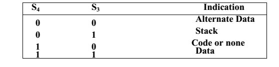
The S4 and S3 combinedly indicate which segment register is presently being used for memory accesses as in below fig.These lines float to tri-state off during the local bus hold acknowledge. The status line S6 is always low.
The address bit are separated from the status bit using latches controlled by the ALE signal.
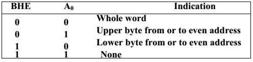
BHE /S7: The bus high enable is used to indicate the transfer of data over the higher order ( D15-D8 ) data bus as shown in table. It goes low for the data transfer over D15-D8 and is used to derive chip selects of odd address memory bank or peripherals. BHE is low during T1 for read, write and interrupt acknowledge cycles, whenever a byte is to be transferred on higher byte of data bus. The status information is available during T2, T3 and T4. The signal is active low and tristated during hold. It is low during T1 for the first pulse of the interrupt acknowledges cycle
RD Read: This signal on low indicates the peripheral that the processor is performing s memory or I/O read operation. RD is active low and shows the state for T2, T3, Tw of any read cycle. The signal remains tristated during the hold acknowledge.
READY: This is the acknowledgement from the slow device or memory that they have completed the data transfer. The signal made available by the devices is synchronized by the 8284A clock generator to provide ready input to the 8086. the signal is active high.
INTR-Interrupt Request: This is a triggered input. This is sampled during the last clock cycles of each instruction to determine the availability of the request. If any interrupt request is pending, the processor enters the interrupt acknowledge cycle.
This can be internally masked by resulting the interrupt enable flag. This signal is active high and internally synchronized.
TEST This input is examined by a ‘WAIT’ instruction. If the TEST pin goes low, execution will continue, else the processor remains in an idle state. The input is synchronized internally during each clock cycle on leading edge of clock.
CLK– Clock Input: The clock input provides the basic timing for processor operation and bus control activity. Its an asymmetric square wave with 33% duty cycle.
MN/ MX : The logic level at this pin decides whether the processor is to operate in either minimum or maximum mode.
The following pin functions are for the minimum mode operation of 8086.
M/ IO – Memory/IO: This is a status line logically equivalent to S2 in maximum mode.When it is low, it indicates the CPU is having an I/O operation, and when it is high, it indicates that the CPU is having a memory operation. This line becomes active high in the previous T4 and remains active till final T4 of the current cycle. It is tristated during local bus “hold acknowledge “.
INTA Interrupt Acknowledge: This signal is used as a read strobe for interrupt acknowledge cycles. i.e. when it goes low, the processor has accepted the interrupt.
ALE – Address Latch Enable: This output signal indicates the availability of the valid address on the address/data lines, and is connected to latch enable input of latches. This signal is active high and is never tristated.
DT/ R – Data Transmit/Receive: This output is used to decide the direction of data flow through the transreceivers (bidirectional buffers). When the processor sends out data, this signal is high and when the processor is receiving data, this signal is low.
DEN – Data Enable: This signal indicates the availability of valid data over the address/data lines. It is used to enable the transreceivers ( bidirectional buffers ) to separate the data from the multiplexed address/data signal. It is active from the middle of T2 until the middle of T4. This is tristated during ‘ hold acknowledge’ cycle.
HOLD, HLDA- Acknowledge: When the HOLD line goes high, it indicates to the processor that another master is requesting the bus access.
The processor, after receiving the HOLD request, issues the hold acknowledge signal on HLDA pin, in the middle of the next clock cycle after completing the current bus cycle.
At the same time, the processor floats the local bus and control lines. When the processor detects the HOLD line low, it lowers the HLDA signal. HOLD is an asynchronous input, and is should be externally synchronized.
If the DMA request is made while the CPU is performing a memory or I/O cycle, it will release the local bus during T4 provided:
- The request occurs on or before T2 state of the current cycle.
- The current cycle is not operating over the lower byte of a word.
- The current cycle is not the first acknowledge of an interrupt acknowledge sequence.
- A Lock instruction is not being executed.
The following pin function are applicable for maximum mode operation of 8086.
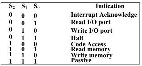
S2, S 1, S0 – Status Lines: These are the status lines which reflect the type of operation, being carried out by the processor. These become activity during T4 of the previous cycle and active during T1 and T2 of the current bus cycles.
LOCK This output pin indicates that other system bus master will be prevented from gaining the system bus, while the LOCK signal is low.
The LOCK signal is activated by the ‘LOCK’ prefix instruction and remains active until the completion of the next instruction. When the CPU is executing a critical instruction which requires the system bus, the LOCK prefix instruction ensures that other processors connected in the system will not gain the control of the bus.
The 8086, while executing the prefixed instruction, asserts the bus lock signal output, which may be connected to an external bus controller.
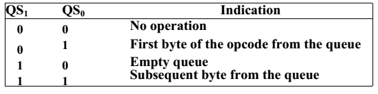
QS1, QS0 – Queue Status: These lines give information about the status of the code-prefetch queue. These are active during the CLK cycle after while the queue operation is performed.
This modification in a simple fetch and execute architecture of a conventional microprocessor offers an added advantage of pipelined processing of the instructions.
The 8086 architecture has 6-byte instruction prefetch queue. Thus even the largest (6 – bytes) instruction can be prefetched from the memory and stored in the prefetch. This results in a faster execution of the instructions.
In 8085 an instruction is fetched, decoded and executed and only after the execution of this instruction, the next one is fetched. By prefetching the instruction, there is a considerable speeding up in instruction execution in 8086. This is known as instruction pipelining.
At the starting the CS:IP is loaded with the required address from which the execution is to be started. Initially, the queue will be empty an the microprocessor starts a fetch operation to bring one byte (the first byte) of instruction code, if the CS:IP address is odd or two bytes at a time, if the CS:IP address is even.
The first byte is a complete opcode in case of some instruction (one byte opcode instruction) and is a part of opcode, in case of some instructions ( two byte opcode instructions), the remaining part of code lie in second byte.
The second byte is then decoded in continuation with the first byte to decide the instruction length and the number of subsequent bytes to be treated as instruction data.
The queue is updated after every byte is read from the queue but the fetch cycle is initiated by BIU only if at least two bytes of the queue are empty and the EU may be concurrently executing the fetched instructions.
The next byte after the instruction is completed is again the first opcode byte of the next instruction. A similar procedure is repeated till the complete execution of the program.•The fetch operation of the next instruction is overlapped with the execution of the current instruction. As in the architecture, there are two separate units, namely Execution unit and Bus interface unit.
While the execution unit is busy in executing an instruction, after it is completely decoded, the bus interface unit may be fetching the bytes of the next instruction from memory, depending upon the queue status.
RQ / GT0 , RQ / GT1 – Request/Grant: These pins are used by the other local bus master in maximum mode, to force the processor to release the local bus at the end of the processor current bus cycle. Each of the pin is bidirectional with RQ/GT0 having higher priority than RQ/GT1.RQ/GT pins have internal pull-up resistors and may be left unconnected.
Request/Grant sequence is as follows:
- A pulse of one clock wide from another bus master requests the bus access to 8086.
- During T4(current) or T1(next) clock cycle, a pulse one clock wide from 8086 to the requesting master, indicates that the 8086 has allowed the local bus to float and that it will enter the ‘hold acknowledge’ state at next cycle. The CPU bus interface unit is likely to be disconnected from the local bus of the system.
- A one clock wide pulse from the another master indicates to the 8086 that the hold request is about to end and the 8086 may regain control of the local bus at the next clock cycle. Thus each master to master exchange of the local bus is a sequence of 3 pulses. There must be at least one dead clock cycle after each bus exchange.
- The request and grant pulses are active low.
- For the bus request those are received while 8086 is performing memory or I/O cycle, the granting of the bus is governed by the rules as in case of HOLD and HLDA in minimum mode.