Microprocessor – Instruction Format And Addressing Mode
INSTRUCTION FORMAT:
All instruction of 8085 are 1 to 3 bytes in length .the bit pattern of the first cycle is the op code. The bit pattern is decoded in the instruction register and p[provides information used by the timing and content section to generate sequence of elementary operation micro operation that implemented the instruction.
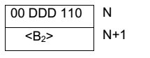
Figure shows a single –byte instruction is the opcode of the instruction. The 8-bit of the op-code available at the memory location N is divided into three potion first group D7, D6 recent group D5D4D3 and third group D2D1D0, D2D1D0 when necessary contains the same code SSS. D2D1D0 group contain the combination of register DDD. If a register pair is involved the bits. RP is placed in D5D4. Whenever D5D4 represents the register pair D3 normal tells whether it is loading operation or storing operation .the first group D7, D6 gives the idea of the mnemonic of the operation code.
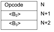
Whenever 8-byte instruction is used the first byte at memory N is the op-code of the instruction followed by either an 8-bit data or an 8-bit address at memory location N+1.
Whenever a 8-byte instruction is in solved .the first byte at memory location N is the opcode followed by either a-16 bit address or a 16-bit data. The second memory location U (N+1).contain the lower order addresses or data and (n+2) contain the higher order address or data
ADDRESSING MODES:
Most of the instruction executes requires two operands e.g. transfer of data between two register of a microprocessor system. How the Mp knows the position of these operands. The method of identifying the operands position by the instruction format is known as the addressing mode. Whenever two operands are involved in an instruction the first operand is assumed to be in a register Mp itself.
It is for the user to put that operand may be located in one of the following.
i. In any general purpose register in the .
ii. In a particular memory location.
iii. It can be immediately available in an instruction format.
iv. I/O device.
In 8085 the following addressing modes are used.
When the operands for any instruction are available in the internal general purpose register. Only the register need be specified as the address of the operands. Such instruction are said to be use the register addressing mode. These instruction are one byte instruction within that byte i.e. OP code, the register are specified.
E.g., MCV r1, r2, ADD r, XCHG, DAD rp etc.
MOVr1, r2 this is an ALP statement and memory of the instruction is more the content of reg (2) to register r1 .the opcode for the instruction is 01DDD SSS .DDD specifies. The code for the operation register (r1) and specifies the code for transfer the first two bits 01 specify the MOV operates MOV B, A the opcode 01 000 111=47H.
ADD r: This is an ALP statement ADD is the mnemonic for addition and meaning of the instruction is add the content of the register to the content of the accumulator and store the result back in accumulator .the one of the operand is assumed to be in accumulator. By implied addressing mode the second operand is available in any general purpose register specified in the instruction .the op code is 10 000 SSS.
E.g. ADD H. The opcode is 10 000 100=84, the macro ITL is implemented. (A) (A) +(r)
Direct addressing mode:
In the addressing mode, the instruction contains the address of the operand contains the address of the operand (external register) involved in the transfer. The 8085A provides.16-bit memory addresses requiring that the address contained in the instruction 1b 16-bit long as a second their byte of the instruction thus it is invariably eg.3-byte instruction.
E.g. LDA addr. This is an ALP statement ADDR in operand field is a symbolic name given to 16-bit address .the systematic name given to 16-bit address symbolic name can be chosen by the user either reference to context LDA is the mnemonic for LOAD accumulator direct. The instruction format for this is as shown.
Where the memory location ‘N’ contains the opcode namely 00 110 010=(3A)4 followed by a lower order 8-bits of address and higher order 8-bit of address at memory location NH&N+2 respectively. The meaning of instruction is load the accumulator from the memory location whose address is available directly, in the instruction itself. The macro RTL implemented is,
(A) M(B3,B2)
This is symbolic representation. Only one operand is involved in the instruction e execution.
Register indirect addressing:
The instruction specifies a register pair which contains the address of the memory. Where the data is located or into which the data in to be placed these, the address of the operand is given indirectly through a register pair. In other words, the operand is in memory location or external register share address is available in an internal general purpose register pair.
The H8L register pair is used as a pointer in memory 8885 A, register indirect instruction .the reg H holds the high and reg L holds the large bytes of the effective address e.g. MOV r, M transfer single bytes from an external reg. M to any of the several integral varying register. External reg M means the external reg pointed by HL the macro RTL implemented is,
(r) M (H, L)
Before reg indirect instruction are used in a program, a previous instruction most load register pair HL with the appropriate address.
The register pair BC & DE is also used as pointer register in two 8085A instructor i.e. LDAX & STAX rp .the internal register involved for data transfer is always accumulator.
The meaning of LDAX rp is load the accumulator from the memory location. Whose address is available in rp (reg pair either BC or DE). The macro RTL implemented is, the opcode for LDAX B is 00 001 010 = (0A).
Immediate Addressing Mode:
In the type of addressing mode, the operand is available directly in the instruction itself. If the operand data involved is of 8-bits then the instruction is of two bytes. The first byte is the opcode followed by 8-bit data. If 16-bit data is involved in the instruction then the first byte is opcode at memory location N followed by the lower data at memory location NH and higher order data at memory location N+2.
e.g. MVI r, data there is two byte instruction .the instruction format is
The meaning of the instruction is more the 8-bit data immediately available in the instruction as the 2nd byte to the destination reg r. DDD identifies the internal register the macro RTL implanted
i.e., (r) <– <B2>
Implied addressing mode:
There are certain instructions that operate on one operand in the ACC and therefore need not specify any address. Many instructions in the logics group like RLC, RRC, RAR, RAL, CMA fall in to the category. All these are one byte instruction .these instruction that specify the address the operand is implied addressing for the other operand.
INSTRUCTION SET
Classification of instruction set:
The 74 instructions available in the 8085A can be divided into
five groups depending on their function.
1. Data transfer group: Instruction that more data between registers,
between register and memory location and I/O transfer.
2. Arithmetic group: Instructions that add subtract increment or
decrement data in the register.
3. Logic group: Instruction that carry out logic operation, such an AND,
OR, EX-OR compare between and data in the accumulator & a
register compliment and rotate data in the accumulator.
4. Branch group: Instruction that change .the execution sequence of a
program, such as conditional and unconditional jump instruction and
subroutine call and return instruction.
5. Stack machine control group: Instruction for maintaining the stack
and internal control flags.
DATA TRANSFER GROUP:
It consists of 15 basic operation and 86 variations. The basic operation involved is DATA transfer between two register of a microprocessor system.
One of the register is always located in the micromprocessor itself the other may be located in one of the following
1) An I/o device
2) Memory
3) The microprocessor
Registers located in the microprocessor are referred to as internal registers. (A, A, C, D, E, H, L, SP, PC) and those in ROM ,RWM, or I/O are referred to as external registers therefore, this group includes transfer of data from reg to mg, Reg to memory, memory to reg. Reg (a) to output devices, or from input device to reg (A).
The register from which data in transfers is the source register and the register to which data is transferred in the destination register. A transfer involves copying the contents of the source reg into the destination register; the contents of the source register and not attend. Each data transfer instruction identifies the source register and the destination register. Identification of one or both of these register may be implied by the instruction in memories or may be explicit. Internal registers are frequently implied; whereas the external registers are usually identified by an explicit address that is part of the instruction.
Data Transfer Group Instructions
- MOV r1, r2 (Move Data; Move the content of the one register to another). [r1] <– [r2]
- MOV r, m (Move the content of memory register). r <– [M]
- MOV M, r. (Move the content of register to memory). M <– [r]
- MVI r, data. (Move immediate data to register). [r] <– data.
- MVI M, data. (Move immediate data to memory). M <– data.
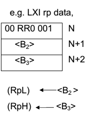
- LXI rp, data 16. (Load register pair immediate). [rp] <– data 16 bits, [rh] <– 8 LSBs of data.
- LDA addr. (Load Accumulator direct). [A] <– [addr].
- STA addr. (Store accumulator direct). [addr] <– [A].
- LHLD addr. (Load H-L pair direct). [L] <– [addr], [H] <– [addr+1].
- SHLD addr. (Store H-L pair direct) [addr] <– [L], [addr+1] <– [H].
- LDAX rp. (LOAD accumulator indirect) [A] <– [[rp]]
- STAX rp. (Store accumulator indirect) [[rp]] <– [A].
- XCHG. (Exchange the contents of H-L with D-E pair) [H-L] <–> [D-E].
ARITHMETIC GROUP:
This group perform the arithmetic operation on the operands normally the operands are necessary for any arithmetic operation one of the operand is always seen in the accumulator the other operand can be seen in one of the three positions.
(a) an internal general purpose register (r)
(b) In a memory location pointed by M pointer (H, L) pair.
(c) Immediately in the instruction itself as a 2nd byte.
All of the flags are effected as per standard rule.
There are 20 basic instructions in this group.
- ADD r. (Add register to accumulator) [A] <– [A] + [r].
- ADD M. (Add memory to accumulator) [A] <– [A] + [[H-L]].
- ADC r. (Add register with carry to accumulator). [A] <– [A] + [r] + [CS].
- ADC M. (Add memory with carry to accumulator) [A] <– [A] + [[H-L]] [CS].
- ADI data (Add immediate data to accumulator) [A] <– [A] + data.
- ACI data (Add with carry immediate data to accumulator). [A] <– [A] + data + [CS].
- DAD rp. (Add register paid to H-L pair). [H-L] <– [H-L] + [rp].
- SUB r. (Subtract register from accumulator). [A] <– [A] – [r].
- SUB M. (Subtract memory from accumulator). [A] <– [A] – [[H-L]].
- SBB r. (Subtract register from accumulator with borrow). [A] <– [A] – [r] – [CS].
- SBB M. (Subtract memory from accumulator with borrow). [A] <– [A] – [[H-L]] – [CS].
- SUI data. (Subtract immediate data from accumulator) [A] <– [A] – data.
- SBI data. (Subtract immediate data from accumulator with borrow). [A] <– [A] – data – [CS].
- INR r (Increment register content) [r] <– [r] +1.
- INR M. (Increment memory content) [[H-L]] <– [[H-L]] + 1.
- DCR r. (Decrement register content). [r] <– [r] – 1.
- DCR M. (Decrement memory content) [[H-L]] <– [[H-L]] – 1.
- INX rp. (Increment register pair) [rp] <– [rp] – 1.
- DCX rp (Decrement register pair) [rp] <– [rp] -1.
- DAA (Decimal adjust accumulator) .The instruction DAA is used in the program after ADD, ADI, ACI, ADC, etc instructions. After the execution of ADD, ADC, etc instructions the result is in hexadecimal and it is placed in the accumulator. The DAA instruction operates on this result and gives the final result in the decimal system. It uses carry and auxiliary carry for decimal adjustment. 6 is added to 4 LSBs of the content of the accumulator if their value lies in between A and F or the AC flag is set to 1. Similarly, 6 is also added to 4 MSBs of the content of the accumulator if their value lies in between A and F or the CS flag is set to 1. All status flags are affected. When DAA is used data should be in decimal numbers.
LOGICAL GROUP:
It consists of 19 basic instructions. There are three basic logic operation AND XOR & OR logical operation takes place bit by. The operand is assumed to be in the accumulator. The second operand is seen either in the internal general purpose register, in the memory location pointed to the M- pointer or as the second byte logical operation is stored back in the accumulator
- ANA r. (AND register with accumulator) [A] <– [A] ^ [r].
- ANA M. (AND memory with accumulator). [A] <– [A] ^ [[H-L]].
- ANI data. (AND immediate data with accumulator) [A] <– [A] ^ data.
- ORA r. (OR register with accumulator) [A] <– [A] v [r].
- ORA M. (OR memory with accumulator) [A] <– [A] v [[H-L]]
- ORI data. (OR immediate data with accumulator) [A] <– [A] v data.
- XRA r. (EXCLUSIVE – OR register with accumulator) [A] <– [A] v [r]
- XRA M. (EXCLUSIVE-OR memory with accumulator) [A] <– [A] v [[H-L]]
- XRI data. (EXCLUSIVE-OR immediate data with accumulator) [A] <– [A]
- CMA. (Complement the accumulator) [A] <– [A]
- CMC. (Complement the carry status) [CS] <– [CS]
- STC. (Set carry status) [CS] <– 1.
- CMP r. (Compare register with accumulator) [A] – [r]
- CMP M. (Compare memory with accumulator) [A] – [[H-L]]
- CPI data. (Compare immediate data with accumulator) [A] – data.The 2nd byte of the instruction is data, and it is subtracted from the content of the accumulator. The status flags are set according to the result of subtraction. But the result is discarded. The content of the accumulator remains unchanged.
- RLC (Rotate accumulator left) [An+1] <– [An], [A0] <– [A7],[CS] <– [A7].The content of the accumulator is rotated left by one bit. The seventh bit of the accumulator is moved to carry bit as well as to the zero bit of the accumulator. Only CS flag is affected.
- RRC. (Rotate accumulator right) [A7] <– [A0], [CS] <– [A0], [An] <– [An+1].The content of the accumulator is rotated right by one bit. The zero bit of the accumulator is moved to the seventh bit as well as to carry bit. Only CS flag is affected.
- RAL. (Rotate accumulator left through carry) [An+1] <– [An], [CS] <– [A7], [A0] <– [CS].
- RAR. (Rotate accumulator right through carry) [An] <– [An+1], [CS] <– [A0], [A7] <– [CS]
Branch Group
The branching instructions alter normal sequential program flow, either unconditionally or conditionally. The unconditional branching instructions are as follows:
JMP Jump
CALL Call
RET Return
Conditional branching instructions examine the status of one of four condition flags to determine whether the specified branch is to be executed. The conditions that may be specified are as follows:
NZ Not Zero (Z = 0)
Z Zero (Z = 1)
NC No Carry (C = 0)
C Carry (C = 1)
PO Parity Odd (P = 0)
PE Parity Even (P = 1)
P Plus (S = 0)
M Minus (S = 1)
Thus, the conditional branching instructions are specified as follows:
- JZ addr (label). (Jump if the result is zero)
- JNZ addr (label) (Jump if the result is not zero)
- JC addr (label). (Jump if there is a carry)
- JNC addr (label). (Jump if there is no carry)
- JP addr (label). (Jump if the result is plus)
- JM addr (label). (Jump if the result is minus)
- JPE addr (label) (Jump if even parity)
- JPO addr (label) (Jump if odd parity)
Stack, I/O and Machine Control Group
- IN port-address. (Input to accumulator from I/O port) [A] <– [Port]
- OUT port-address (Output from accumulator to I/O port) [Port] <– [A]
- PUSH rp (Push the content of register pair to stack)
- PUSH PSW (PUSH Processor Status Word)
- POP rp (Pop the content of register pair, which was saved, from the stack)
- POP PSW (Pop Processor Status Word)
- HLT (Halt)
- XTHL (Exchange stack-top with H-L)
- SPHL (Move the contents of H-L pair to stack pointer)
- EI (Enable Interrupts)
- DI (Disable Interrupts)
- SIM (Set Interrupt Masks)
- RIM (Read Interrupt Masks)
- NOP (No Operation)
For Offline Study you can Download from below link
Download Microprocessors Instruction Format And Addressing Mode PDF File