Microprocessor – Memories and IO Interfacing
IO Interfacing INPUT/OUTPUT Techniques
In all process content applications, Microprocessor would like to communicate with different I/O devices for data transfers is transfer of data between circuitry external to the Microprocessor itself. This transfer of data is in addition to transfers between the microprocessor and memory and is referred to as input/output or I/O.
In addition to the memory and keyboard interfaced to the Microprocessor many input & output peripheral devices may have to be interfaced with the system to obtain a micro-computer depending upon a particular control applications same of the input devices interfaced are push bottom switches, toggle switches, a TTY, CRT, analog to digital converters etc. some of the output devices interfaced are LED s, seven segment displays, TTY, CPT, printers, digital to analog converters etc.
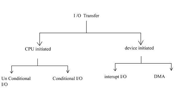
In the case of CPU initiated I/O transfer, it is the Microprocessor which through a software initiates the action of data transfer. In the case of device initiated it is the external device which is interested in communication with CPU initiates the data transfer operation. The CPU initiated I/O transfer is also known as program controlled I/O, because the transfer of data is completely under the control of the microprocessor program. An I/O operation takes place only when an I/O transfer instruction is encountered in the execution of the program.
This I/O transfer may be unconditional or conditional I/O transfer. In the case of CPU initiated unconditional I/O transfer CPU initiates the data transfer and assumes that the external device is always ready to input a data into the Microprocessor at the time of data transfer initiated by the Microprocessor and therefore microprocessor affects the transfer of data through corresponding instructions.(toggle switches).In the case of an output data transfer the Microprocessor assumes that the output device is already to accept data and sends the necessary data through the corresponding instructions
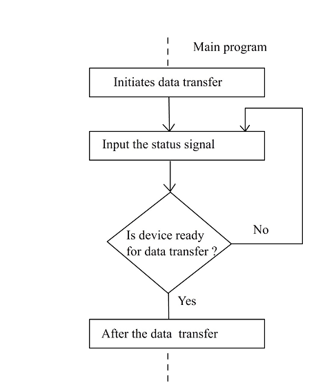
In the case of CPU initiated polled I/O transfer, again it is the CPU that initiates the data transfer operation but it does not assume that the peripheral device is ready for data transfer.flip flop checks the readiness of the device before the data transfer occurs. This involves testing one or more status flags or bits associated with the I/O device before the data transfer .this is known as hand shake control signals .the flow chart for CPU initiated polled I/O transfer is shown in fig.
CPU initiated polled I/O transfer can be preferred if and only if the Microprocessor has no other useful work to do in the process control under consideration and can wait away the ti9me till the device is ready for data communication. On the other hand, if the wait away time is large like 1 sec or 1min and the process control application under consideration demands some useful work to be done by the Microprocessor.
In such cases, CPU initiated polled I/O transfer shall be dispensed with and device initiated I/O transfer should be preferred.
Device initiated I/O transfer is one which the device initiates the transfer of data. There are two main of data transfer;
In the case of device initiated interrupt I/O transfer (also known as interrupt program controlled I/O), an external device indicates directly to the Microprocessor its readiness to transfer data by making the corresponding interrupt control signal active. Most Microprocessor interrupted input can be disabled u8nder program controlled I/O. when a microprocessor program is interrupted, Microprocessor recognizes the fact that the external device has requested for the data transfer & control is transferred to an interrupt service subroutine.
This subroutine performs the data transfer and then return the control to the program at the point it was interrupted, and processing continues thus, with an interrupt program controlled I/o operation, the data transfer is requested by an external device and then implemented by an interrupt service subroutine.
D.M.A stands for direct memory access.flip flop is also referred to as hardware controlled I/O, flip flop is the only type of I/O transfer in which the Microprocessor is not involved in the transfer of data between the memory and the external device .
In this case there is direct data transfer between an I/O device and memory, data Is not transferred from an I/O device to one of the Microprocessor registers and then to memory a vice-versa. In DMA,Microprocessor goes to the HOLD state. the address bus data and the data communication control signal like RD BAR ,WR BAR , .IO/M BAR are all tri-stated and the external device which initiates the D.M.A through making HOLD control signal active, takes the command of the address bus BDB and BCB and The control signal for data transfer applications between the memory & device DMA is used primarily to transfer a number of words or black of data at high speed.
Interfacing IO Devices
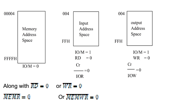
As discussed earlier, input port and output port are basically external registers. The IO/M BAR control signal of the 8085 A determines whether the address generated during a data transfer refers to memory IO/M BAR =0 IO/M BAR=1
Address space is truth divided by control strobes into an input address space RD BAR=o and an output address space WR BAR=0 Fig shows how the address space of 8085 A is partitioned by this control signal. When I/O ports are assigned separate address space distinct from the address space of the external register that comprise main memory (other than memory space), they are referred to as isolated or standard I/O.
Only the IN and OUT instructions provide data transfer for isolated I/O IN and OUT each require three m/c cycles for execution the first is of course, an OPCODE FETCH. The second is MEMORY READ during which the 8-bit port address is transferred from memory to the p and placed in both the W & Z temporary registers and the third is either an I/O READ on I/O WRITE machine cycle during which the actual data transfer from or to the I/O device occurs. During the I/O READ and I/O WRITE m/c cycles, the 8-bit port address, in W & Z is outputted from the 8085 A on address data bus lines AD7-AD0 and on address lines AD15-AD8,8.the read (RD BAR) and write (WR BAR) control strobes from the 8085 A specify the exact time at which an input port’s tri-state buffer is enabled to drive the data bus or the exact time at which an output port the data placed on the data bus by the microprocessor respectively.
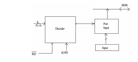
For input ports, external decoding logic combines RD BAR, IO/M BAR , and the port address and generates a unique input device select pulse for each input port. The pulse occurs only during the I/O READ m/c cycle of an in interaction that address the specific port. The input device select pulse enables the input port’s tri-state buffer.2f through design or program error. The tri-state buffers of two or more ports or a port and a memory device are simultaneously enabled both drive the data bus and cause bus contention.
For output operation, external decoding logic combines WR BAR , IO/M BAR and the port address and generates a unique output device select pulse occurs only during the I/O WRITE m/c cycle of an OUT instruction that addresses the port and decks the output port’s register. Typically each output device select pulse checks a single output port; however it is possible that more than one port are selected simultaneously.
Memory Mapped I/O :
In this cases the I/O devices are not given separate addresses other than memory i.e. 0000 to FFFF.(64k).but part of the space is reserved for I/O devices. The advantage is any instruction that references memory can also transfer data between an I/O device and the Microprocessor ,as long as the I/O port is assigned to the memory address space rather than to the I/O address space. The register associated with the I/O port is simply treated as memory location register.
Consider an example in which address bit A15 designates whether instructions reference memory or an I/O device.2f A15= 0, a memory register is addressed; If A15= 1, than a memory mapped I/O device is address .this assignment elevates the first 32kbytess of memory address space to memory and second 32k to memory mapped I/O devices. External logic generates devices select pulses for memory mapped I/O only when IO/M BAR= 0, the appropriate address is on the address low and a RD BAR or WR BAR strobe occurs.
Input and output transfer using memory mapped I/O are not limited to the accumulator. For example, same of 8085 A instructions that can be used for input from memory mapped I/O ports
MOV r, m move the connects of input port whose address is available in (H,L) reg pair to any internal register.
LDA addr load the acc with the content of the input port whose address is available as a second and third byte of the instruction.
Other instructions include, ANA M, ADD M, 1HD add (input from two ports and store the contents is reg pair (L) and (H) ADD M and ANA M provide input data transfer and computation in a single instruction. same instruction that out the data from memory mapped ports are
MOV M,r
STA addr
MVI M, data
SHLD addr
LHLD and SHLD carry out 16- bit I/O transfers with single instructions which reduce program executive time considerably. The price paid for this added capability is a reduction in directly addressable main memory and the necessity of decoding a 16- bit rather than an 8-bit address.
When a microprocessor puts out an address and generates a control strobe for a memory read, it has no way of determining whether the device that responds with data is a memory device or an I/O device; nor does it care. If only requires that the devices that respond does so with in the allowable access time or uses the READY line to request a sufficient number of WAIT states.
The some of true when a Mircoprocessor executives a write to memory.2f supplies an address data, and a write strobe and continues its operations, external logic determines whether memory, I/O or anything at all receives the data transferred.