Digital Electronics – Clocked S-R Flip-Flop
Generally, synchronous circuits change their states only when clock pulses are present. The operation of the basic flip-flop can be modified by including an additional input to control the behavior of the circuit. Such a circuit is shown below:-
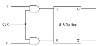
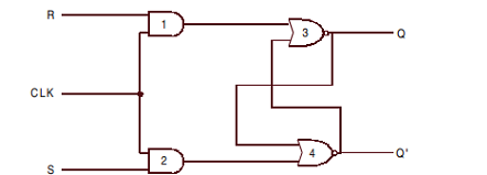
The circuit shown above consists of two AND gates. The clock input is connected to both of the AND gates, resulting in LOW outputs when the clock input is LOW. In this situation the changes in S and R inputs will not affect the state (Q) of the flip-flop. On the other hand, if the clock input is HIGH, the changes in S and R will be passed over by the AND gates and they will cause changes in the output (Q) of the flip-flop. This way, any information, either 1 or 0, can be stored in the flip-flop by applying a HIGH clock input and be retained for any desired period of time by applying a LOW at the clock input. This type of flip-flop is called a clocked S-R flipflop. Such a clocked S-R flip-flop made up of two AND gates and two NOR gates is shown in Figure below:-
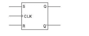
The logic symbol of the S-R flip-flop is shown below. It has three inputs: S, R, and CLK. The CLK input is marked ith a small triangle. The triangle is a symbol that denotes the fact that the circuit responds to an edge or transition at CLK input.
Assuming that the inputs do not change during the presence of the clock pulse, we can express the working of the S-R flip-flop in the form of the truth table shown here. Here, Sn and Rn denote the inputs and Qn denotes the output during the bit time n. Qn+1 denotes the output after the pulse passes i.e. in the bit time n + 1.
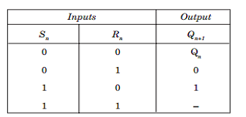
Case 1. If Sn = Rn = 0, and the clock pulse is not applied, the output of the fl ip-fl op remains in the present state. Even if S n = Rn = 0, and the clock pulse is applied, the output at the end of the clock pulse is the same as the output before the clock pulse, i.e., Qn+1 = Qn. The first row of the table indicates that situation.
Case 2. For S n = 0 and Rn = 1, if the clock pulse is applied (i.e. CLK = 1), the output of NAND gate 1 becomes 1; whereas the output of NAND gate 2 will be 0. Now a 0 at the input of NAND gate 4 forces the output to be 1 i.e. Q’ = 1. This 1 goes to the input of NAND gate 3 to make both the inputs of NAND gate 3 as 1, which forces the output of NAND gate 3 to be 0, i.e., Q = 0.
Case 3. For S n = 1 and Rn = 0, if the clock pulse is applied (i.e., CLK = 1), the output of NAND gate 2 becomes 1; whereas the output of NAND gate 1 will be 0. Now a 0 at the input of NAND gate 3 forces the output to be 1, i.e., Q = 1. This 1 goes to the input of NAND gate 4 to make both the inputs of NAND gate 4 as 1, which forces the output of NAND gate 4 to be 0, i.e., Q’ = 0.
Case 4. For Sn = 1 and Rn = 1, if the clock pulse is applied (i.e. CLK = 1), the outputs of both NAND gate 2 and NAND gate 1 becomes 0. Now a 0 at the input of both NAND gate 3 and NAND gate 4 forces the outputs of both the gates to be 1, i.e., Q = 1 and Q’ = 1. When the CLK input goes back to 0 (while S and R remain at 1), it is not possible to determine the next state, as it depends on whether the output of gate 1 or gate 2 goes to 1 first.