Digital Electronics – Latches and Flipflops
FLIPFLOPS
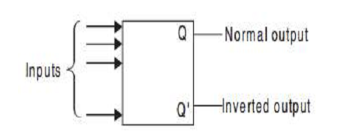
The basic 1-bit digital memory circuit is known as a flip-flop. It can have only two states, either the 1 state or the 0 state. A flip-flop is also known as a bistable multivibrator. Flip-flops can be obtained by using NAND or NOR gates. The general block diagram representation of a flip-flop is shown in Figure below.
It has one or more inputs and two outputs. The two outputs are complementary to each other. If Q is 1 i.e., Set, then Q’ is 0; if Q is 0 i.e., Reset, then Q’ is 1. That means Q and Q’ cannot be at the same state simultaneously. If it happens by any chance, it violates the definition of a flip-flop and hence is called an undefined condition. Normally, the state of Q is called the state of the flip-flop, whereas the state of Q’ is called the complementary state of the flipflop. When the output Q is either 1 or 0, it remains in that state unless one or more inputs are excited to effect a change in the output.
Since the output of the flip-flop remains in the same state until the trigger pulse is applied to change the state, it can be regarded as a memory device to store one binary bit. The block diagram of a flipflop is given below:-
LATCHES
The basic difference between a latch & flip-flop is, Storage elements that operate with signal levels (rather than signal transitions) are referred to as latches; those controlled by a clock transition are flip-flops. Latches are said to be level sensitive devices; flip-flops are edge-sensitive devices.
The two types of storage elements are related because latches are the basic circuits from which all flip-flops are constructed.
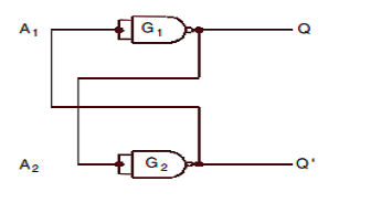
We consider the fundamental circuit shown in Fig.(last page). It consists of two inverters G1 and G2 (NAND gates are used as inverters). The output of G1 is connected to the input of G2 (A2) and the output of G2 is connected to the input of G1 (A1).
Let us assume the output of G1 to be Q = 0, which is also the input of G2 (A2 = 0). So, the output of G2 will be Q’= 1, which makes A1 = 1 and consequently Q = 0 which is according to our assumption. Similarly, we can demonstrate that if Q = 1, then Q’ = 0 and this is also consistent with the circuit connections.
Hence we see that Q and Q’ are always complementary. And if the circuit is in 1 state, it continues to remain in this state and vice versa is also true. Since this information is locked or latched in this circuit, therefore, this circuit is also referred to as a latch. In this circuit there is no way to enter the desired digital information to be stored in it.
To make that possible we have to modify the circuit by replacing the inverters by NAND gates and then it becomes a flip-flop.